The Tail of Two Footprints
In today's story we are going to talk about the importance of checking your footprints and datasheets before you finalize your design. And more importantly, if you're going to substitue a part, make sure you check the footprint of the part you're going to use for any differences. This is a story of a simple mistake that cost me a run of PCBs and weeks of time on the project.
The Setup
I was working on a new design for a PCB that has around 20 addressable LEDs on it. Many people know these as Adafruit's NeoPixels. I needed the component in my parts library so I went to digikey to see if they had ECAD models and such and... they do!
![]()
So I happily pulled them into my parts library and started designing my schematic and laying out the board. I had a looming deadline so I was in a hurry to get the layout done and sent off to the fab house. I was so excited to get this board back and start testing it out.
The Problem
I use JLCPCB assembly whenever possible because I work on very dense boards and without a pick-n-place machine, I can't really do the 0402 parts without a lot of headache. This board was no different. I had finished the design and the ERC and DRC were passing with no errors. It was time to create the gerbers, bom, and pnp files. When I got to the JLCPCB assembly phase, they don't have the Adafruit 1655 LEDs. What they do have is, what I thought was the underlying part that Adafruit uses, the SK6812 by Optoelectronics (part number OSK-SPC-SK6812-012). A quick look at the datasheet reveals that it speaks the same protocol and has the same footprint. Plus the linked Adafruit datasheet references a similar part number: "OSK-SPC-SKC6812RV". Easy enough, substitue the in-stock part and move on right? WRONG!
Let's review the datasheets
Adafuit OSK-SPC-SKC6812RV datasheet
The first thing you'll notice is that the non-Adafruit datasheet is in chinese. This makes it hard to read when you don't know the first thing about the language. But more importantly, it means that I can only skim the pages and look for key things that "match" or "don't match". I typically only care about the protocol and the footprint key dimensions when doing last mile substitutions.
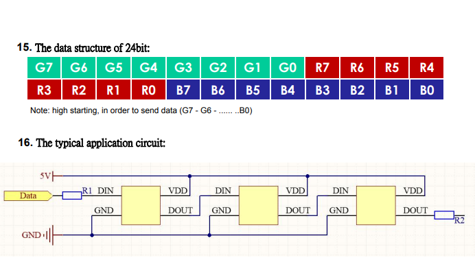
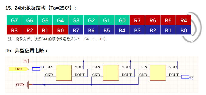
Protocol
Adafruit Version

Generic Version

So those look the same... Plus the part numbers seem to support this.
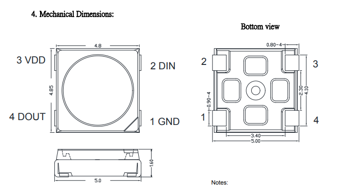
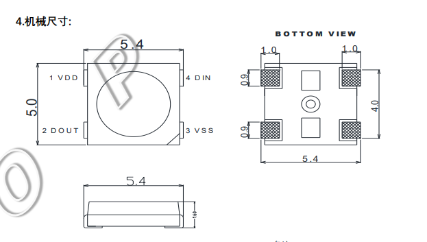
Footprint Size
Adafuit Version

Generic Version

Slightly different but the pad configuration in my library allows for the dimensional differences. These will fit and the pads will line up.
That's it right? We are good, swap it in and call it a day... Some of you may have caught it, I certainly did not.
Wait, What?
Look again at the pin numbers. The pin positions are the same, ie: VSS is the notched pin, and VDD is the top right, etc, but look at the numbers!
Pin 1 in the Adafruit part is ground but on the generic its VDD!
Now, some of you will probably say, what does it matter, they are the same in terms of layout relative to the notch. To that I respond, yes but the pick-n-place doesn't know that! Also, I didn't put an outline silk screen on the footprint that shows the notch, I just put a dot next to pin 1.
If you put "pin 1" to the dot, you have flipped the part in the assembly!
- Is this something I could have caught on my layout check on JLCPCB? Yes, but I didn't expect the pin numbers to be different.
- Is this something I could have caught on my final assembly check? Yes, but, again, I checked the dot to pin one in my libary which has the Adafruit footprint.
- Is this an easy mistake? Absolutely!
- Is the fix just as easy? Yes! Make sure you treat substitute parts at the final phase the same as your design phase... READ THE DATASHEET CAREFULLY
- Will checking pinout and footprint orientation be part of my substitution checks now? Until the end of time.
- Can I just rework them on my bench to fix the boards? Yes... its 20 per board, so it took me quite a long time.
Conclusion
In conclusion, I urge you to learn from this mistake. The one key takeaway is to ALWAYS CHECK ALL KEY ELEMENTS OF THE DATASHEET!. From now on my substitution checklist will include, "pin out numbering to layout".
Thanks for reading and I wish you all perfect PCBs with no bodges required in the New Year!
If you'd like to submit your own Engineering Hell stories, we'd love to publish them: Share your Story
